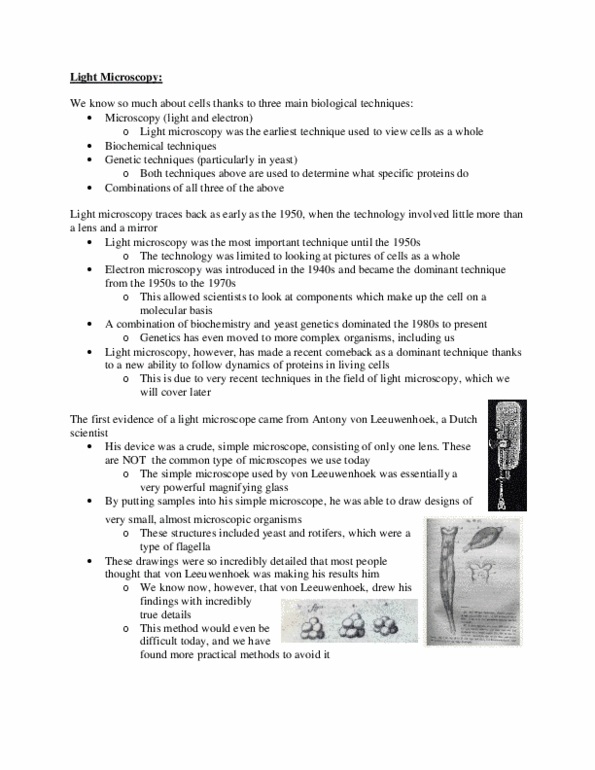
Electron Microscopy:
To get a sense of scaling for electron microscopy, lets start by looking at someones finger,
about 20mm across, and then zoom into a spot by 10x every time
1X the whole finger is visible 20mm
10X the skin can be seen close up as ridges 2mm
100X the skin layers can roughly be seen (low mag.
LM) 0.2mm
1000X start seeing distinct cells and some organelles
(very high power LM) 20 microns
10KX details of organelles 2 microns
100KX large complexes become visible from a low
mag. 0.2 microns
1MX Individuals ribosomes can be seen (and other
macromolecular complexes) 20nm
10MMX atoms becomes visible (atomic resolution)
2nm
100MX individual atoms can be seen 0.2nm
LM, as we saw before, has a resolving power of about 200nm, at which point cells like bacteria
(1 micron) begins to look like dots
Techniques like X-Ray NMR are used for atomic resolution to give detailed structural
biology at the level of Angstroms (1A is 0.1nm)
o NMR becomes impractiral, though, for looking at larger molecules and complexes
Therefore, to fill the gap between LM and NRM, theres electron microscopy, EM, for
which there are different types
o While EM is not good for atomic resolution, it can be used to look at things
smaller than 200nm
The limit of resolution, d, is the smaller distance between two objects with which they can still
be distinguished
It can be calculates using the formula to the right,
and is dependent on three things:
o The angle of the rays collected by the
objective lens; this value can maximize at
a value of 1
o n is the refractive index of the medium between the specimen and, usually
o The wavelength of light is directly proportional to d, and is often the factor we
play around with to try and change the resolving power
Typically in LM, we use the visible spectrum of light as a lambda value, from about 400-
700 nm
o For EM, much smaller values are used
In EM, the wavelength of electrons is dependent on voltage; we typically use a voltage
of 100kV, which gives a lambda of 3.7 x 10 nm
o This would produce, in theory, a resolution limit of about 0.002nm, which is
100,000 time that of LM =12
o However, a modern EM at about 300kV with lambda approx. equal to 2.2 x 10
m will only have a resolution of about 1A, 0.1nm, because only the very center of
the lens can be used as the aperture
The first electron microscope was built in 1931by Ernst Ruska and Max Knollat the Berlin
Technische Hochschule
Although this crude initial instrument was capable of magnifying objects by 400X, it
demonstrated the principles of an electron microscope
o This was more a proof of concept than as an effective machine
Two years later, Ruska constructed an electron microscope that exceeded the resolution
possible with an optical microscope
It was greatly developed through the 1950sand has allowed great advances in the natural
sciences and physics
The advantage of an electron beam is that it has a much smaller wavelength, which
allows a higher resolution-the measure of how close together two things can be before
they are seen as one
o Light microscopes allow a resolution of about 200nm, whereas electron
microscopes can have resolutions as low as 0.1 nm (1A)
EM can commonly be used to try and answer the following things:
Morphology and changes in morphology caused by certain diseases (i.e. whats going
wrong in the cell)
Protein localization and trafficking, and thus the mistargeting and mislocating caused by
disease
Understanding protein function which can allow us to, for example, develop drug which
prevent bacterial ribosome function (disease prevention)
There are two main types of EM: transmission EM, or TEM, and scanning EM, or SEM
TEM is used for infrastructural components and has more versatile applications, and has
a high resolution than SEM
SEM is used mainly for topographical information, and not for detailed work on cell
infrastructure
LM, SEM, and TM do have a similar design and serve similar purposes; to make small things
bigger for us to see them
In LM, the light source comes from a
light, but in EM, electrons are produced
from a heated filament
Instead of glass lenses, EM techniques
used magnetic coils to condense and
magnify the electron beam
o In TEM, the sample is placed
right after the condenser, like an
LM, and the electrons pass
through it (everything is
analogous to LM)o In SEM, the sample is located at the bottom after a series of lenses, and electrons
are scattered off of it
A beam deflector allows you to move the electron beam and literally scan
along the sample surface
The bouncing pattern of the electrons is recorded on a viewing screen,
now usually a computer
In all EM, electrons can collide with air particles, so the process must take place inside a
vacuum
o Presence of air will cause the image to blur
There are different types of interactions between the
electrons and the sample depending on the type of EM
used
The source of light comes from the incident high
kV electron beam which comes from the heated
filament
All EMs experience some background noise
which can come from backscattered electrons
(BSE), Characteristic X-Rays, visible light,
inelelastically scattered electrons and Bremsstrahlung X-rays
TEM uses elastically scattered electrons in comparison with direct beams, which both go
through the sample
SEM uses secondary
More
Less