CSE 220 Lecture 11: Circuits and K-maps

3 Mar 2017
School
Department
Course
Professor
Document Summary
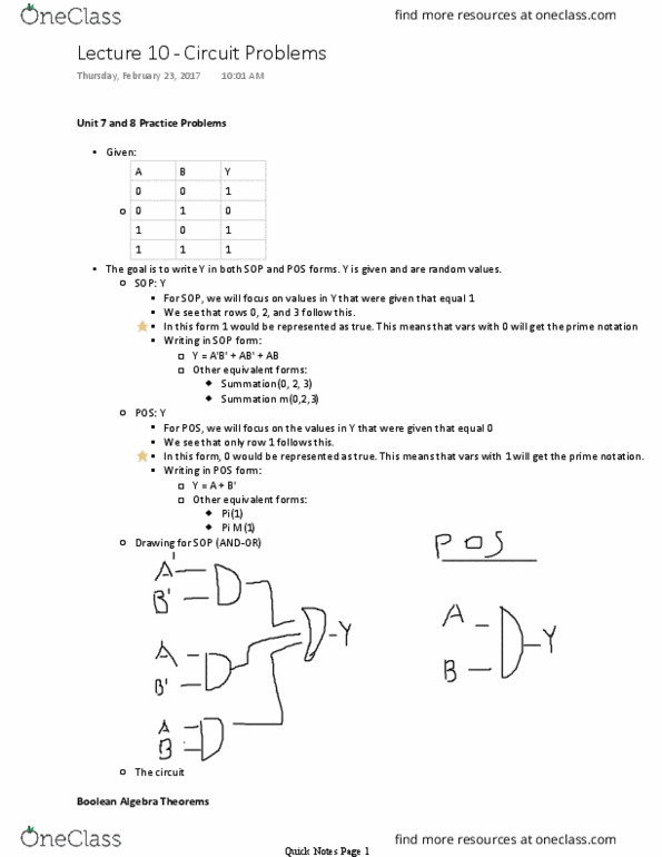
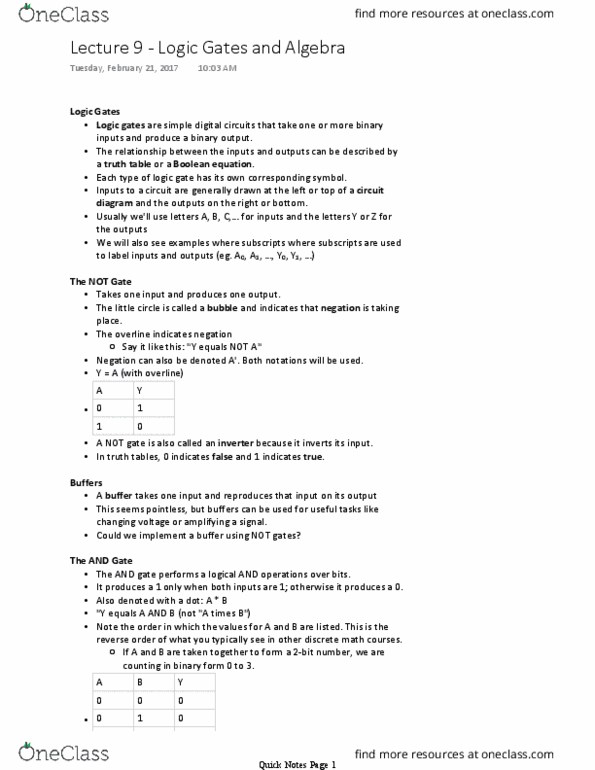
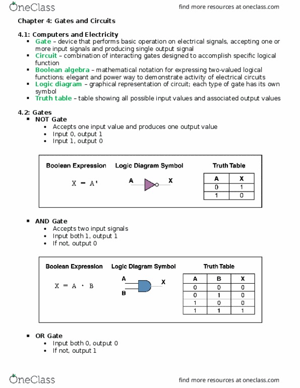
So far we have seen two-level combination logic circuits in sum of products and product of sums forms. Sometimes we can make a simpler circuit if we use more than two levels of gates. Also, sometimes the sop or pos forms are more complicated than an alternative form. In practice, integrated circuit manufacturers prefer to use nand or nor gates instead of and and or gates to make circuits because these gates require fewer transistors than and and or gates. Thus, nand and nor gates use less space than and and or gates and so more can be packed on a chip. However, circuits made entirely of nand or nor gates can be hard to understand when written as boolean equations or as a circuit diagrams. A procedure called bubble pushing can help us transform a circuit diagram into one that is easier to interpret. Specifically, de morgan"s law allow us to push bubbles through gates, either forward or backward.