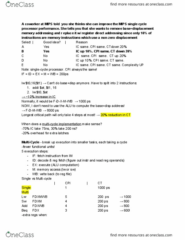
Help SOS SOS
MIPS Pipeline
You will implement a five-stage MIPS pipeline, which is the most common organization for
MIPS and is similar to what is described in the textbook and in class:
1. Fetch
2. Decode
3. Execute
4. Memory
5. Writeback
What to Implement
Implement a five-stage pipelined MIPS processor using VHDL. Your design should contain a
program counter (PC), a Instruction memory (I RAM), Data memory (D RAM), a register file,
ALU, and any other components needed, along with the instruction decode and control circuits
needed to connect them all together. The pipeline should: fetch instructions to execute from the
program RAM and increment the program counter by 4; decode each instruction; select
arguments from the register file; compute results; do memory access if the instruction is LW or
SW; and store results back in the register file.
Your pipeline must correctly execute all of the instructions in the following table 1:
Immediate arithmetic Addi, Andi, Ori, Slti
Register arithmetic Add, Sub, And, Or, Slt, Xor
Shift Sll, Srl
Memory LW, SW
Data Hazard: The trivial solution to data hazards is, of course, stalling. However, the
performance of trivial solutions is not optimal. Implement forwarding such that your
implementation will handle data hazards without sacrificing performance.
Extra Credit
Implementing the functionality of the instructions in table 2
Jump J, JR, JAL
Branches Beq, Bne, Blez
Testing
Write a testbench program in MIPS assembly that fully tests all of the features you have
implemented. This is a critical step, and you should spend a fair amount of time developing a
comprehensive program that exercise all of the different instructions and features of your processor. The program should be well commented, indicating what it is doing and what results
should be expected when running the program, so that the course staff is convinced of the
correctness of your processor.
Documentation
The design document should include a block diagram showing all the major components in the
processor (ALU, Register File, PC, pipeline registers, etc.), and the datapath connections
between them. You need not completely draw wires for control logic signals, but should indicate
which components take control inputs, and give names to all control signals. Overall, the
diagram should be very similar to (and not much more complicated than) the diagrams used in
lecture, but with labels for control signals and any relevant data signals. You should provide an
explanation for any parts of your processor or any subcomponents that are unusual or potentially
confusing.
Also include a description of your control and instruction decoding logic. For each control logic
signal (or group of related control logic signals) you should provide (a) a brief description of
what the signal does, e.g. what the values of the control signal mean; and (b) a truth table
showing what value the signal takes for each possible opcode.
What to Submit
• A VHDL project file containing your processor and all needed subcomponents.
• A VHDL file containing your well-commented MIPS assembly testbench program.
• A design document of your processor.
Academic Integrity. As one of the most widely studied architectures, MIPS has a wealth of
information available on the web and in textbooks. You may consult any MIPS documentation
available to you in order to learn about the instruction set, what each instruction does, etc. But
we expect your design to be entirely your own, and your submission should cite any significant
sources of information you used.
References