24 Nov 2021
Department
Course
Professor
Document Summary
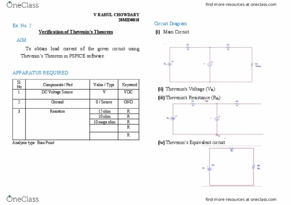
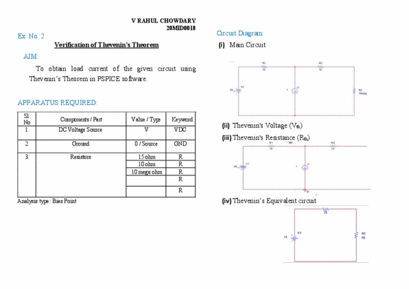
Design & simulation of half and full adder circuits. To perform the half adder and full adder operation using logic gates in pspice simulation. Keyword: digital clock, ground, xor gate ic, and gate ic, or gate ic. Half adder is a combinational circuit that performs the addition of two bits, this circuit needs two binary inputs and two binary output. The implementation of half adder using exclusive or and an and gates is shown in circuit diagram. Full adder is a combinational circuit that performs the addition of three bits (two significant bits and previous carry). It consists of three inputs and two outputs, two inputs are the bits to be added, the third input represents the carry form the previous position. The full adder is usually a component in a cascade of adders, which add 8, 16, etc, binary numbers. The implementation of full adder using exclusive or, and, and or gates is shown in circuit diagram.