EECE 144 Lecture Notes - Lecture 10: Sequential Logic, Sequential Circuits, Addition

26 Jun 2018
School
Department
Course
Professor

Chapter 4 Notes: Combinational Logic
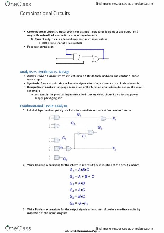
● Combinational Circuits
○ Made from an interconnection of logic gates.
Chapter 5 Notes: Synchronous Sequential Logic
● Sequential Circuits
○ Reacts to values of signals at inputs to produced wanted output signal
○ Input and outputs variables are physically analog signal whose values are
interpreted to be binary signal that represents logic 1 and logic 0
○
○ ** if registers are in circuit, then its a sequential circuit
○ For every n input variable, there are 2^n possible combinations of binary inputs.
● Analysis Procedure
○ Analysis → find the functions
■ Given the logic diagram with boolean functions, truth table, or explanation
of circuit
1. Make sure given circuit is combinational (meaning no feedback paths or
memory elements)
Feedback path: connection from output of one gate to input of second gate
whose output forms part of input to first gate
2. Obtain output boolean functions
● Design Procedure
1. Determine required number of inputs and outputs
2. Derive truth table
3. Find simplified boolean functions
4. Draw logic diagram and verify correctness
★ Binary Adder-Subtractor
○ Half Adder
■ Addition of two bits
■ INPUT = augend(x) and addend(y) bits
■ OUTPUTS = sum(S) and carry(C)
Document Summary
Made from an interconnection of logic gates. Reacts to values of signals at inputs to produced wanted output signal. Input and outputs variables are physically analog signal whose values are interpreted to be binary signal that represents logic 1 and logic 0. ** if registers are in circuit, then its a sequential circuit. For every n input variable, there are 2^n possible combinations of binary inputs. Given the logic diagram with boolean functions, truth table, or explanation of circuit: make sure given circuit is combinational (meaning no feedback paths or memory elements) Feedback path: connection from output of one gate to input of second gate whose output forms part of input to first gate. Design procedure: determine required number of inputs and outputs, derive truth table, find simplified boolean functions, draw logic diagram and verify correctness. Addition of three bits (two bits and a carry) Two half adders make a full adder.