MATS 3011 Lecture Notes - Charge Density, Depletion Region, Meke

Document Summary
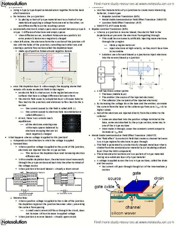
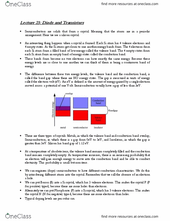
=acceptor type atom junction btwn p type and n type semiconducting materials. If + charge tries to go to right, will have opposing forcesame for electronthis is why you don"t deplete everything. Region @ interface where holes and electrons eat each other up = depletion region. Matsci page 1 built-in potential (barrier for movement of electrons and holes) -> barrier for motion of electrons and holes (charge movement) decreases picture above becomes. Current vs voltage from p-n diode reverse bias forward bias. Idea behind photodiode: have semiconductor w/ certain band gap reverse bias. -> shine a light --> create holes and electrons --> use device to separate holes and electrons --> creates current. Photodiode is a p-n junction operated in reverse bias to separate electrons and holes, which are created by photons if light shined is greater than band gap, then you flow a current upon exposure of light.