ELE 747 Lecture Notes - Lecture 8: Fourier Series, Douglas Dc-8, Voltage Source

9 Apr 2016
School
Department
Course
Professor
Document Summary
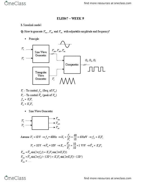
4. 3 pulse width modulation (pwm) cv mv ov. 1ov t mv - modulating wave (sine) cv - carrier waver (triangular) m vv , m f f c c. Peak voltage of modulating and carrier waves. Number of pulses per half cycle ov - output voltage waveform of. 1ov - fundamental component of ov: modulation index dm. A: adjust dm cv mv t ov mf. 1a max dm na - amplitude of the nth harmonic ma1 - maximum amplitude of fundamental component d. 1 d no low order harmonics over modulation na low order harmonics start to appear. 1 dm: to reduce harmonics, to avoid non-linearity. 4. 4 - 3 voltage source inverters (vsi) (1) circuit diagram o. V a is not defined, dependant on the load (not allowed!!) (3) square wave operation (3) waveforms (180 conduction angle) 2g are complimentary gate signals (2) av is determined by bv is determined by cv is determined by.